Semiconductors and the India Semiconductor Mission: Fab Incentives, How Chips Are Made, and ISM Facts for UPSC GS3
In one line: The India Semiconductor Mission (ISM), launched in December 2021 under MeitY with a Rs 76,000 crore outlay, is India’s flagship programme to build a complete chip ecosystem — design, fabrication, and packaging — and this page gives you the full story in exam-ready form.
- What is the India Semiconductor Mission (ISM)? – Lead Answer
- What Are Semiconductors? Basic Physics in Plain English
- How a Chip Is Made: From Sand to Wafer
- Design, Fabrication and ATMP: The Chip Value Chain
- Why Fabs Cluster Geographically: Taiwan, South Korea, and the US
- ISM Schemes: Fab Incentives and Display Manufacturing
- Design Linked Incentive (DLI) and SPECS Schemes
- Approved Projects: Tata fabs in Dholera and Assam, Micron ATMP
- ISRO-Style Indigenous Chips: Semiconductor Laboratory (SCL) Mohali
- Why Semiconductors Matter for India: Strategic and Economic Angle
- Challenges for India’s Chip Ambitions
- Prelims and Mains Quick Facts + Memory Hooks
- Frequently Asked Questions
- Q: When was the India Semiconductor Mission launched and under which ministry?
- Q: What percentage of project cost does the government provide for semiconductor fabs under ISM?
- Q: What is the difference between a fab and an ATMP unit?
- Q: How is ISM linked to ISRO chips?
- Q: Why is this topic important for UPSC GS3?
- Related reading
In one line: Read the lead answer first, then the value chain and how-chips-are-made sections, then the schemes and approved projects, and finish with the Prelims facts and Mains skeleton at the end.
This page fixes the entire ISM topic permanently. UPSC has a habit of framing semiconductor questions as either pure science (GS3 science and technology) or pure policy (industry incentives and supply chains). Examiners love the trap pair: how chips are physically made versus why India struggles to make them. You need both halves, and you need them connected. That connection is exactly what this article builds.
What is the India Semiconductor Mission (ISM)? – Lead Answer
The India Semiconductor Mission is a dedicated programme announced by the Government of India in December 2021 with a total outlay of Rs 76,000 crore. It is implemented by the Ministry of Electronics and Information Technology (MeitY) through a dedicated division called India Semiconductor Mission. Its objective is not just to attract one factory — it is to build a complete, sustainable semiconductor and display ecosystem in India: chip design, wafer fabrication, assembly-testing-marking-packaging (ATMP), and display manufacturing. Memorise the trio — 2021, MeitY, Rs 76,000 crore — because every Prelims question on ISM begins there.
What Are Semiconductors? Basic Physics in Plain English
A semiconductor is a material whose electrical conductivity lies between a conductor (copper) and an insulator (rubber). The workhorse material is silicon, extracted from sand — the second most abundant element in Earth’s crust. Silicon’s usefulness comes from a property called “doping”: deliberately adding tiny amounts of impurity atoms to change its conductivity.
- N-type silicon: doped with phosphorus or arsenic — extra electrons (negative carriers) are added.
- P-type silicon: doped with boron — electron “holes” (positive carriers) are created.
- P-N junction: where p-type meets n-type, you get a diode — current flows one way only. Stack junctions and you get transistors, the switches that compute.
A modern chip contains billions of transistors packed onto a thumbnail-sized piece of silicon. The “nanometre” label you read in the news (28nm, 14nm, 5nm) refers loosely to how small and tightly packed these transistors are — smaller means faster, cooler, and more power-efficient.
How a Chip Is Made: From Sand to Wafer
Understand this as a six-step assembly line. Examiners test whether you can order these steps correctly.
- Purification: Sand (silica) is refined into ultra-pure polysilicon — 99.9999999% (“nine nines”) purity. This is why metallurgical-grade silicon alone cannot make chips.
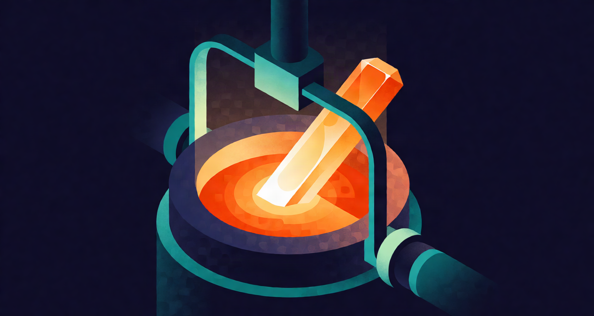
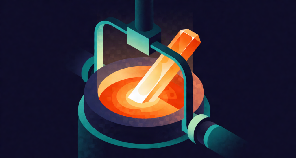
- Ingot growth: Pure polysilicon is melted and a single-crystal silicon ingot (a cylindrical boule) is grown using the Czochralski process.
- Wafer slicing: The ingot is sliced into thin wafers (typically 200mm or 300mm diameter), then polished to a mirror finish.
- Photolithography: Light is projected through a mask onto photoresist-coated wafers, printing circuit patterns at nanometre scale. Extreme ultraviolet (EUV) lithography machines from ASML (Netherlands) are the world’s most advanced — and export-controlled.
- Etching and doping: Exposed material is etched away, and doping (ion implantation) is used to create the p-type and n-type regions of each transistor. This cycle of lithography–etch–dope repeats dozens of times, layer upon layer.
- Packaging: The finished wafer is cut into individual dies, tested, and packaged into the black plastic chips that go onto circuit boards. This stage is ATMP/OSAT work.
Design, Fabrication and ATMP: The Chip Value Chain
Stop treating “chip company” as one thing. The industry is split into three segments, and this distinction is the most examined pair in this topic:
- Fabless design companies: Design chips but outsource manufacturing — e.g., Nvidia, Qualcomm, and India’s own strong design base.
- Foundries (fabs): Manufacture wafers for others — e.g., TSMC (Taiwan), Samsung (South Korea). This is the most capital-intensive step: a leading-edge fab costs $10–20 billion.
- ATMP / OSAT: Assembly, Testing, Marking and Packaging — Outsourced Semiconductor Assembly and Test. Less capital-intensive, more labour-tolerant — which is why India’s first approved projects (Micron, Tata Assam) sit here.
Why Fabs Cluster Geographically: Taiwan, South Korea, and the US
TSMC alone fabricates a majority of the world’s leading-edge chips, nearly all of it in Taiwan. This concentration is not an accident — it is explained by four factors, and this is a classic Mains point:
- Capital intensity: A single advanced fab costs billions, with heavy subsidies (US CHIPS Act, EU Chips Act, China’s Big Fund).
- Water and power: Fabs run 24/7 and consume enormous quantities of ultrapure water and stable electricity.
- Skilled talent: Process engineers with decades of accumulated know-how.
- Supplier ecosystem: Equipment, gases, chemicals, and materials suppliers cluster around fabs, creating lock-in.
This clustering is also why chip supply chains are a geopolitical vulnerability — one chokepoint in the Taiwan Strait can freeze global auto and electronics production, as the 2020–22 shortage showed.
ISM Schemes: Fab Incentives and Display Manufacturing
Under ISM, the central government provides fiscal support of up to 50% of the eligible project cost for:
- Semiconductor fabs (silicon wafer manufacturing);
- Display fabs;
- Compound semiconductors (using materials like silicon carbide and gallium nitride — critical for EVs, power electronics, 5G) and semiconductor packaging (ATMP/OSAT) facilities.
Several states (Gujarat, Assam, Uttar Pradesh, Odisha) offer additional top-ups on top of the central 50%. This PLI-style design — matching a share of project cost rather than output-linked payouts — is deliberate: fabs need huge upfront capital before a single chip is sold.
Design Linked Incentive (DLI) and SPECS Schemes
Two supporting schemes complete the picture:
- Design Linked Incentive (DLI): Provides financial incentives and design infrastructure support to semiconductor design startups — up to 50% of eligible expenditure, plus access to EDA tools and foundry access through the ChipIN Centre at C-DAC Bengaluru. India’s strength here is real: a figure MeitY cites regularly — roughly a fifth of the world’s chip designers are Indian.
- SPECS (Scheme for Promotion of Manufacturing of Electronic Components and Semiconductors): A production-linked incentive of 4–6% on incremental sales for manufacturers of electronic components, sub-assemblies, and semiconductors — feeding the broader ecosystem around chips.
Approved Projects: Tata fabs in Dholera and Assam, Micron ATMP
In February–March 2024, the Union Cabinet approved the first batch of ISM projects. These four names are Prelims gold:
- Tata Electronics + PSMC (Taiwan): A semiconductor fab at Dholera, Gujarat — India’s first commercial silicon fab, targeting 28nm-and-above nodes.
- Tata Electronics: An ATMP (assembly and test) unit at Morigaon, Assam.
- CG Power + Renesas (Japan): An OSAT facility in Sanand, Gujarat.
- Micron (US): An ATMP/testing and packaging unit at Sanand, Gujarat — the first ISM project announced, in June 2023.
Notice the pattern: three of the four are packaging units, only one is a fab. That tells you exactly where India sits in the value chain today — entering through ATMP while building toward fabrication. Learn this pattern; it is a ready-made Mains observation.
ISRO-Style Indigenous Chips: Semiconductor Laboratory (SCL) Mohali
Long before ISM existed, India’s only government-owned fab was the Semiconductor Laboratory (SCL) at Mohali, Punjab, established in the 1980s. SCL fabricates chips for ISRO satellites and strategic/defence applications, working with older, radiation-hardened process nodes suited to space-grade electronics. Its modernisation — and technology transfer to commercial players like Tata Electronics — is part of the indigenous chip push. For Prelims, remember: ISM covers commercial fabs; SCL Mohali is the strategic/ISRO-linked fabrication asset.
Why Semiconductors Matter for India: Strategic and Economic Angle
Connect these four threads for GS3:
- Import dependence: India imports essentially all its chips — electronics imports rival oil in value.
- Supply chain resilience: The 2020–22 global chip shortage disrupted Indian auto and electronics manufacturing.
- Strategic needs: Defence systems, missiles, satellites, telecom (5G), and EVs all run on chips — linking GS3 science-tech to internal security.
- Economic ambition: India’s electronics manufacturing target ($300 billion by 2026) cannot hold without a domestic chip base — linking to Make in India, PLI, and National Policy on Electronics 2019.
Challenges for India’s Chip Ambitions
A balanced Mains answer names the obstacles honestly:
- Capital intensity: Even with 50% support, private investors hesitate over long payback periods and cyclical demand.
- Water and power: Fabs need lakhs of litres of ultrapure water daily — site selection (Dholera, Sanand) reflects this.
- Talent gap: India has designers but few process engineers with fab operating experience.
- Thin ecosystem: Lack of local suppliers for gases, chemicals, and equipment keeps costs high.
- Subsidised competition: Rivals in the US, China, EU, Taiwan and Korea receive far larger, longer-standing state support.
Prelims and Mains Quick Facts + Memory Hooks
Read these one-liners once tonight and once before the exam.
- Launched: December 2021 | Outlay: Rs 76,000 crore | Ministry: MeitY
- Fab incentive: up to 50% of project cost (fabs, display, compound semiconductors, ATMP)
- DLI: chip design startup incentives; SPECS: components manufacturing PLI
- Key names: Tata–PSMC Dholera fab; Tata Assam ATMP; CG–Renesas OSAT; Micron Sanand
- SCL Mohali: ISRO and strategic chip fabrication
- Memory hook: “76 for chips in ’21” — Rs 76,000 crore, 2021, MeitY.
Mains skeleton (150 words): (1) Context: global chip shortage + import dependence. (2) ISM design: Rs 76,000 crore, 50% fab support, DLI, SPECS. (3) Progress: Tata Dholera fab, Assam ATMP, Micron Sanand. (4) Challenges: capex, water, talent, ecosystem. (5) Way forward: ATMP-first entry, design strength, SCL modernisation, skilling — conclude on strategic autonomy.
For authoritative detail, consult the official programme page at MeitY, ISM India, and the Semiconductor Industry Association’s global supply chain reports at semiconductors.org.
Frequently Asked Questions
Q: When was the India Semiconductor Mission launched and under which ministry?
ISM was announced in December 2021 with a Rs 76,000 crore outlay and is implemented by the Ministry of Electronics and Information Technology (MeitY) through ISM as a dedicated division.
Q: What percentage of project cost does the government provide for semiconductor fabs under ISM?
Up to 50% fiscal support for eligible fab, display, and compound semiconductor projects, with several states offering additional top-ups on top of the central share.
Q: What is the difference between a fab and an ATMP unit?
Fabs manufacture silicon wafers using photolithography — extremely capital-intensive. ATMP units handle assembly, testing, marking and packaging of finished dies — far less capital-intensive, which is why India’s first approved projects are largely ATMP facilities.
Q: How is ISM linked to ISRO chips?
The Semiconductor Laboratory (SCL) at Mohali fabricates chips for ISRO satellites and strategic sectors. Modernising SCL and transferring its technology to commercial players forms part of India’s indigenous chip capability push alongside ISM.
Q: Why is this topic important for UPSC GS3?
It sits at the junction of science and technology, industry policy (incentives and PLI-style support), supply chain resilience, and internal security — a single topic that lets you answer questions across the entire GS3 spectrum.
Related reading
- Socio-Religious Reform Movements of 19th Century India: Leaders, Organisations and Years Mapped for Exams
- Governor-General vs Viceroy of India: Powers, Reforms and Acts — Tabulated Comparison for Exams
Quick revision
- N-type silicon: doped with phosphorus or arsenic — extra electrons (negative carriers) are added.
- P-type silicon: doped with boron — electron “holes” (positive carriers) are created.
- P-N junction: where p-type meets n-type, you get a diode — current flows one way only. Stack junctions and you get transistors, the switches that compute.
- Purification: Sand (silica) is refined into ultra-pure polysilicon — 99.9999999% (“nine nines”) purity.
- Ingot growth: Pure polysilicon is melted and a single-crystal silicon ingot (a cylindrical boule) is grown using the Czochralski process.
- Wafer slicing: The ingot is sliced into thin wafers (typically 200mm or 300mm diameter), then polished to a mirror finish.
Have a doubt on this topic?