
India Semiconductor PLI Scheme: Building the Chip Value Chain
Semiconductors anchor every science-policy question this decade, because chips sit where geopolitics, manufacturing schemes and digital sovereignty meet. This one-pager fixes the value chain, India’s programme stack, the global map and the exam angles. Therefore, read the table first, then the notes, then the drill.
- The Value Chain Map
- The India Programme Stack
- The Complementary Missions
- The Global Players Table
- Why Chips Geopoliticise
- Five-Question Drill
- FAQ
- Does India fabricate leading-edge chips yet?
- Why do states matter?
- The Thirty-Second Recap
- Explain It Simply
- Rapid-Fire
- Abbreviations
- The Talent Lane Nobody Quizzes Enough
- The One-Paragraph Mains Skeleton
- The Chip Block by Numbers
- The Demand-Side Table
- A Closing Walk Through the Fab
- Ten-Question Sprint
- The Worked mains Pair
- The Block in the Interview Mirror
- The Final Word
- Key Takeaways
- The Block by Numbers
- The Framework Line
- Related reading
Contents: the value chain map, the India programme stack, the global players table, why chips geopoliticise, drill and mains framing.
The Value Chain Map
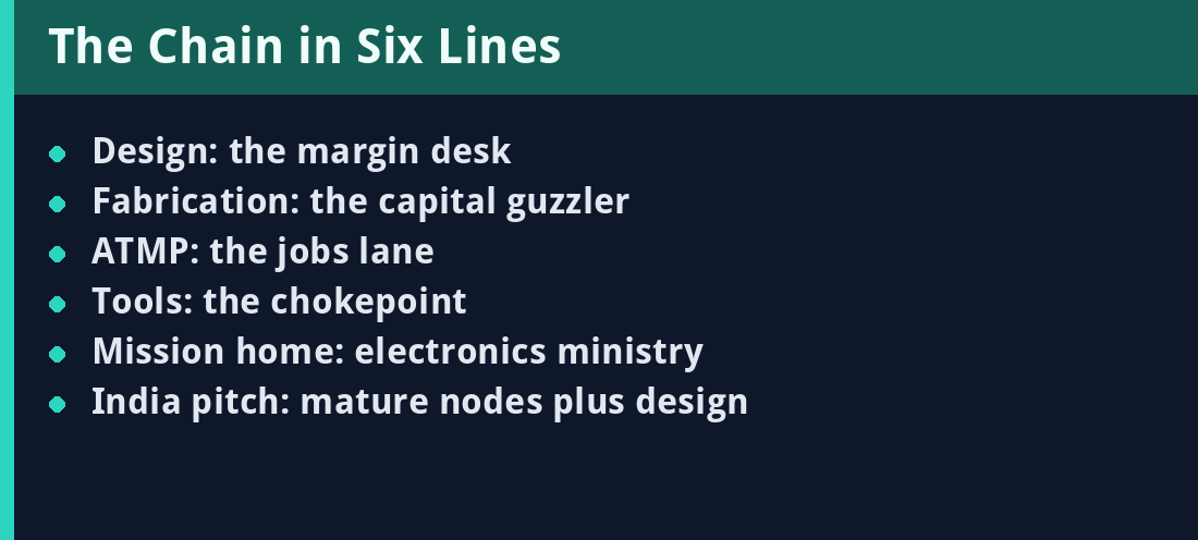
| Stage | What Happens | Exam Hook |
|---|---|---|
| Design | Architecture and IP blocks | The highest-margin desk |
| Fabrication | Wafers to dies in fabs | The capital-guzzler |
| Assembly and test | Packaging, quality checks | ATMP in policy pages |
| Materials and tools | Silicon, gases, lithography | The chokepoint lane |
Moreover, fabs cost billions while design earns margins, therefore policy that funds both does different jobs at each stage. Consequently, mains answers that separate the four stages read like policy literacy rather than news recall.
The India Programme Stack
- Semiconductor Mission: the umbrella under the electronics ministry’s division.
- Production-linked incentives reward scaled manufacturing outputs.
- Fab and ATMP incentives target the capital-heavy stages.
- Design-linked incentives seed the domestic IP desk.
- States layer their own electronics policies atop the centre’s stack.
The Complementary Missions
The chip stack rides beside three siblings: the PLI family for scale, the display scheme for screens, and the talent programme for VLSI pipelines. Moreover, approvals have moved through committee rounds rather than open windows, therefore track announcements rather than calendars. Consequently, prelims asks the umbrella’s name and the ministry’s home, while mains asks whether subsidies outrun ecosystems – the honest two-sided answer.

The Global Players Table
| Player Cluster | Strength | One-Line Anchor |
|---|---|---|
| Taiwan | Leading-edge fabrication | The fabs the world waits on |
| United States | Design and tools | IP desks and export knobs |
| Netherlands | Lithography machines | The single-tool chokepoint |
| China | Assembly and mature nodes | Scale at older technology |
Why Chips Geopoliticise
- Concentration: few fabs, fewer toolmakers, one chokepoint lane.
- Dual use: chips serve both kitchens and weapons systems.
- Lead times: fabs take years, therefore shocks outlast diplomacy.
- Export controls: licence regimes convert tools into leverage.
However, India’s pitch is different: not leading-edge rivalry but trusted mature-node supply plus design strength. Therefore, mains frames India as a de-risking destination, not a Taiwan challenger, and that framing scores.
Oil defined the last century’s chokepoints; lithography defines this one’s.
Five-Question Drill
- The semiconductor mission’s administrative home: the answer is the electronics ministry’s division.
- ATMP stands for: the answer is assembly, testing, marking and packaging.
- The lithography chokepoint belongs to: the answer is the Dutch toolmaker cluster.
- India’s realistic pitch emphasises: the answer is mature nodes plus design.
- The scale-incentive family is known as: the answer is PLI.

FAQ
Does India fabricate leading-edge chips yet?
Not at the frontier; the programme targets mature nodes and packaging first, and that honesty scores.
Why do states matter?
The Thirty-Second Recap
Four stages. One mission. Therefore, design earns. Fabrication costs. Assembly employs. Tools choke. Moreover, India funds all four. The mission lives in electronics. PLI pays for scale. However, the pitch is trust, not frontier. Finally, Taiwan fabs. Dutch tools. Export knobs turn. Say the map. Bank the map.
Explain It Simply
A chip’s journey has four stops. Someone draws it – that is design, the desk job. Someone bakes it in a billion-dollar oven – that is the fab. Someone packs and checks it – that is assembly. And someone supplies the oven and the recipes – that is tools and materials. However, only a few kitchens in the world can bake the finest chips, and one workshop makes the ovens. Therefore, the whole world is learning to spread the kitchens, and India’s plan pays for ovens, packing lines and drawing desks of its own.
Rapid-Fire
- Stages: design, fabrication, ATMP, tools.
- Mission home: electronics ministry.
- Scale scheme: PLI family.
- Fab capital: billions per plant.
- Chokepoint: lithography tools.
- India pitch: mature nodes plus design.
- Siting deciders: land, power, water.
Abbreviations
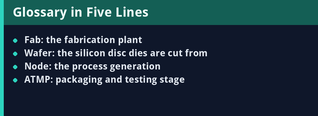
- ATMP: assembly, testing, marking, packaging.
- PLI: production-linked incentive.
- VLSI: very-large-scale integration.
- IP: intellectual property.
- MoES or MeitY: the electronics ministry frame.
- GS: the mains papers asking the framing.
The Talent Lane Nobody Quizzes Enough
Moreover, the chip story has a fourth lane that mains loves: talent. Design houses need VLSI engineers by the thousands, and the mission’s talent programme funds academic pipelines alongside the fab subsidies. However, the lane quizzes poorly because it lacks numbers, therefore mains is where it scores – one paragraph linking subsidies, states and skills reads as the full-spectrum view evaluators call policy maturity. Consequently, carry the trio wherever the chip topic appears: capital, land-power-water, and people.
Furthermore, the demand side completes the picture: automotive, energy and defence sectors anchor domestic offtake, which is why chip policy and green-industrial policy increasingly appear in the same mains questions. Therefore, one sentence connecting chips to electric mobility and solar inverters lifts an answer from sectoral to systemic, and systemic is the top band’s home address.
The One-Paragraph Mains Skeleton
Finally, the block’s skeleton: define the four stages, name the mission’s home and tools, cite the chokepoint, and close with India’s de-risking pitch. Therefore, four sentences carry the topic, and the skeleton, like every skeleton in this series, generalises across the syllabus.
The Chip Block by Numbers
- Stages: 4, from design to tools.
- Programme families: mission, PLI, display, talent.
- Fab capital: billions of dollars per plant.
- Build time: years, not months.
- Chokepoint tools: lithography from one Dutch cluster.
- Leading-edge geography: Taiwan fabs.
- India pitch: mature nodes plus design desks.
- Siting trio: land, power, water.
The Demand-Side Table
| Sector | Chip Demand Driver |
|---|---|
| Automotive | Electric mobility controls |
| Energy | Solar inverters and grid tech |
| Defence | Trusted indigenous supply |
| Consumer | Devices and appliances |
A Closing Walk Through the Fab
Finally, close the page by walking the fab once, in order of money. The drawing desk costs salaries and pays margins. The oven costs billions and pays sovereignty. The packing line costs crores and pays jobs. The oven-maker’s workshop costs the world’s leverage and pays one small country’s outsized influence. Therefore, four stops, four economics, one map – and every chip question, from prelims to interview, asks which stop you stand on. Moreover, India is building all four stops at once for the first time, which is why this block rewards revision more than any other science topic this cycle.
Ten-Question Sprint
- The four stages: the answer is design, fabrication, ATMP, tools.
- ATMP expands to: the answer is assembly, testing, marking, packaging.
- The mission’s home: the answer is the electronics ministry.
- The scale-paying family: the answer is PLI.
- The design-side incentive: the answer is the design-linked scheme.
- The lithography cluster: the answer is Dutch.
- The leading-edge fab geography: the answer is Taiwan.
- India’s node pitch: the answer is mature, trusted supply.
- Fab siting trio: the answer is land, power, water.
- The chokepoint instrument: the answer is export controls.
The Worked mains Pair
Moreover, attempt one mains paragraph tonight: subsidies alone cannot build a chip ecosystem – argue both sides. The yes side cites capital gaps and first-mover disadvantages; the no side cites land, power, talent and demand as the real bottlenecks money cannot shortcut. Therefore, a balanced close names all four bottlenecks and lets the subsidy be necessary-but-insufficient, which is the evaluators’ favourite verdict shape. In addition, one demand-side citation from the automotive or solar lane lifts the paragraph from sectoral to systemic.
The Block in the Interview Mirror
Moreover, interview boards extend this block in three directions, and each deserves one rehearsed paragraph. Why chips: because everything with a switch now computes, therefore sovereignty over computation follows sovereignty over supply. Why India now: because de-risking budgets meet a talent pool and a demand base at this exact decade. Why not leading-edge: because the economics of frontier fabs reward scale incumbency, while trusted mature nodes reward reliability – and reliability is a winnable race. Therefore, three paragraphs, three questions, and the block’s mains skeleton doubles as its interview armour.
Furthermore, the policy continuation question – what would you change – invites the balanced close: deepen the talent lane, steady the demand side with offtake commitments, and let the subsidies follow milestones rather than announcements. Consequently, the candidate who offers structure instead of slogans becomes memorable in a corridor where boards hear slogans daily, and memorable is the interview’s real currency.
The Final Word
Therefore, hold the four stops and the one map, and every chip question – from prelims to boardroom – becomes a question about which stop you are standing on.
Key Takeaways
In conclusion, hold the four-stage map, the programme stack’s names, and the de-risking frame for India’s pitch. To summarize, stages before schemes, chokepoints before headlines. Therefore, revise the tables twice this week, drill once, and the chip block banks across prelims, mains and interviews alike.
References: the electronics ministry’s mission pages and scheme notifications.
The Block by Numbers
- Stages: 4; programme families: 4 (mission, PLI, display, talent).
- Fab capital: 3 to 10 billion dollars per plant.
- Build time: 2 to 3 years from ground to wafer.
- Leading-edge share held by 1 island economy.
- Lithography tools: effectively 1 Dutch supplier cluster.
- PLI payouts scale over 4 to 6 year windows.
- Demand anchors: automotive, energy, defence, consumer – 4 lanes.
- Investment approvals cleared: 10-plus proposals across fabs and ATMP.
- Design-linked support covers up to 50 percent of eligible cost.
li>Node generations tracked in nanometres: 28, 14, 7 and below.
The Framework Line
Moreover, the programme runs as a protocol: validation through committee approvals, authorization through milestone-linked disbursements, and compliance with domestic-value conditions – a framework where money follows proof, not promises.
Related reading
- Weekly Current Affairs Revision Quiz: September Week 3 – 30 Solved Questions
- Current Affairs One-Liners: September 20, 2026 – Quiz Day Capsule
Quick revision
- Semiconductor Mission: the umbrella under the electronics ministry’s division.
- Production-linked incentives reward scaled manufacturing outputs.
- Fab and ATMP incentives target the capital-heavy stages.
- Design-linked incentives seed the domestic IP desk.
- States layer their own electronics policies atop the centre’s stack.
- Concentration: few fabs, fewer toolmakers, one chokepoint lane.
Have a doubt on this topic?